Special Techniques for Matching Multi-band PIFAs
There are several different schools of thought on the question “How should PIFAs be analysed?”, or “How do PIFAs work?”. I’ve found that some of them are useful and some less so, one day I’ll do a series of posts about them.
Right now though, what I’m interested in is the matching, specifically how the ground and feed pins affect it. According to some theories the ground pin plays a role in determining various antenna characteristics. What I’m concerned with here though is it’s role in affecting the input impedance. This part of the theory of PIFA antennas is really quite simple: if the ground pin is close to the feed pin then it forms a shunt inductance to ground. The size of that shunt inductance depends on the thickness and length of the ground pin and the metal between the two pins. So, the ground pin is effectively a matching element, it can be used along with the matching circuit in order to solve the overall matching problem. This is a very useful technique.
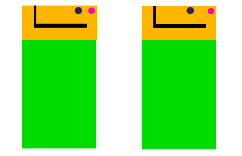
The diagram shows two prototypes for handset PIFA antennas. The groundplane is in green, though I haven’t shown it we’ll suppose that there is a full covering of groundplane below the PIFA area. The PIFA is in yellow, slots cut into the PIFA are in black, the feed pin is marked in blue and the ground pin is marked in pink. These pins could be “pogo” pins from the PCB below up to the PIFA.
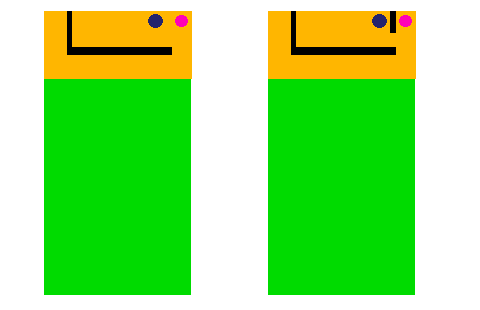
The only difference between these two antennas is the position of the feed and ground pins, this is a big difference though. The smith chart or return loss chart for these two types antennas would be quite different. This is a dual-band design and both bands would be different. Even the antenna patterns would be different. Those are all subjects for another time. From the matching viewpoint the most interesting thing is that the path from the feed pin to ground is longer on the antenna on the right, and shorter on the one on the left. This is a shunt circuit so we should think in terms of admittance. From that view the design on the left has a shunt inductor to ground with higher admittance than the one on the right.
This fact gives the PIFA designer an extra degree of freedom in matching. Let’s suppose the matching circuit is a pi network of three components. Let’s suppose a Smith Chart analysis indicates that a shunt inductor is needed on the side of the pi network connected to the antenna. In that case the designer should think about changing the distance between the feed and ground pin. It is often much easier to change that inductance by altering that distance than by using the matching circuit. But, changing the pin positions also changes the antenna behaviour, making the problem more complicated. This added complexity though produces extra options which can be useful in design.
Often the pin positions are fixed early in a project before the PIFA design is anything like complete. Even in this case though the inductance can be varied by cutting a slot between the ground and feed points. This change will also affect many other characteristics of the PIFA, but it can often be made without difficult mechanical changes. This method can be used to reduce the shunt admittance (or if you prefer increase the shunt reactance), unfortunately there is no similar easy way to raise the shunt admittance.


